OS2 【Open Seminar II 】iNEMI – Large Form Factor Package Assembly
Oct. 21, 2026 15:10 PM - 16:50 PM
Room: TPCA Show Main Stage (Area L, 4F, TaiNEX1)
Session chair: Haley Fu, iNEMI
Panel Level Packaging: Two Very Different Markets
發表編號:OS2-1時間:15:10 - 15:35 |

Invited Speaker
Speaker: E. Jan Vardaman, President, TechSearch International
Bio:
E. Jan Vardaman is president and founder of TechSearch International, Inc., which has provided market research and technology trend analysis in semiconductor packaging since 1987. She is the author of numerous publications on emerging trends in semiconductor packaging and assembly. She is a senior member of IEEE EPS and is an IEEE EPS Distinguished Lecturer and received the Distinguished Achievement Certificate for Technical Leadership and Expertise in May 2024. She received the President’s Award in 2026 from the Global Electronics Association (GEA) for her contributions to the electronics industry. She received the IMAPS GBC Partnership award in 2012, the Daniel C. Hughes, Jr. Memorial Award in 2018, the Sidney J. Stein International Award in 2019, and she is an IMAPS Fellow. She served on the IEEE CPMT Board of Governors for two terms. Before founding TechSearch International, she served on the corporate staff of Microelectronics and Computer Technology Corporation (MCC), the electronics industry’s first pre-competitive research consortium. She
received her M.A. from University of Texas, in 1981.
|
|
Large Form Factor (LFF) Packaging to Enable Heterogenous Integration for AI Era
發表編號:OS2-2時間:15:35 - 16:00 |

Invited Speaker
Speaker: Shripad Gokhale, Senior Principal Engineer, Intel
Bio:
Shripad Gokhale is a Senior Principal Engineer in Advanced Packaging Technology Development at Intel, where he leads early customer engagement and assembly engineering research and development in EMIB scaling for multi‑die, large‑form‑factor chiplet-based systems within Intel Foundry. With over two decades of experience, he has driven architecturally significant packaging innovations spanning heterogeneous integration (EMIB), 3D stacking (Foveros), chip–package interactions, and system‑level thermo‑mechanical and reliability co‑design. His technical leadership was critical to Intel’s first‑generation Foveros enablement and high‑yield EMIB product ramps.
Shripad is an Intel Achievement Award recipient, the author of 18 patents and 20+ technical publications, and a member of Intel’s IP committee. He holds a Ph.D. in Chemical Engineering from Rensselaer Polytechnic Institute and currently leads iNEMI consortium projects on low‑temperature materials and large‑form‑factor packaging—bringing deep, hands‑on design and process leadership at the intersection of chiplet architecture and manufacturable 3D systems.
Abstract:
Increase in global computing demand and artificial intelligence training and inference using large language models is leading to the deployment of advanced packaging technology in volume. Heterogeneous integration of different types of silicon, memory, and other components is very important to realize this demand of 2.5D and 3D packaging. This talk will focus on why LFF packaging is central to the future of heterogeneous integration, from enabling the next generation of AI hardware to reducing costs. It will provide an overview of the Advanced Packaging Technologies needed to enable future Heterogeneous Integrated Products, such as interconnect technologies, thermal challenges, power delivery solutions, manufacturing and yield optimization, etc.
|
|
Next generation LFF (large form factor) IC substrates addressing Advanced Packaging Challenges
發表編號:OS2-3時間:16:00 - 16:25 |

Invited Speaker
Speaker: Venkata Mokkapati, Director, Business Development & Application Engineering, AT&S
Bio:
Venkata Mokkapati is currently leading global Business Development & Application Engineering teams at AT&S AG based in Austria. In this current role as Director, Venkata is involved in Business development for IC substrates & Advanced Packaging, Pricing strategy, F2F customer discussions, Technology portfolio, Technology driving factors and trends, Identifying Disruptive/Alternative/Competitive technologies, Co-ordination and guidance for customer engagements and internal technical developments, Priority setting and direction for technology development needs, Troubleshooting and bridging the business. He is also an expert member for WoW (Ways of Working) and developing internal processes for Strategic marketing, Business Development & Sales processes.
Venkata has more than 18 years of experience in Semiconductor industry and is a certified ICP engineer from Delft University of Technology from where he also holds a PhD. Prior to joining the industry in 2018, Venkata has spent 12 years in academics in various universities/Institutes across Europe and Asia. Venkata also has experience in establishing and running a sole trading company on graphene and other 2D materials. Venkata has authored and co-authored more than 40 peer-review journals/conference proceedings/patents. He is also a recipient of EC-FP7 Marie Curie Co-fund fellowship.
Abstract:
Next-generation Large Form Factor (LFF) IC substrates are emerging as a critical enabler for high-performance computing (HPC), artificial intelligence (AI), and data center applications. As chiplet architectures and heterogeneous integration become industry standards, traditional substrate sizes are no longer sufficient to host increasingly massive multi-die systems. This talk addresses on how LFF substrates address the primary challenges of advanced packaging, including warpage control, thermal management, and the demand for ultra-fine line/space routing. We also would discuss recent advancements in core materials, alongside innovative panel-level manufacturing techniques where the UPP (Unit Per Panel) can be increased.
|
|
Multi-physics Design for Enlarged Chiplets in Advanced Packaging
發表編號:OS2-4時間:16:25 - 16:50 |
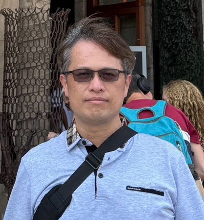
Invited Speaker
Speaker: Joey Huang, Manager, ASE
Bio:
Joey Huang was an electrical engineer at ASE Corporate R&D Electrical Lab. from 2003 to 2018. From 2018 to now, he has been in charge of department of Integration Design at ASE Corporate R&D.
Abstract:
With the increasing demand for HPC/AI applications, HPC/AI computing ICs are moving towards heterogeneous integration, with the increasing integration of chiplets, resulting in larger HPC/AI computing ICs. Furthermore, the speed and bandwidth requirements for chip-to-chip interconnects continue to increase. Advanced packaging must now simultaneously support high-bandwidth memory
(HBM4) and ultra-high-speed UCIe-A interfaces up to 64 Gbps while maintaining electrical integrity, mechanical stability, and manufacturing feasibility. To address these challenges, this paper proposes a multi-physics design approach for larger
chip-to-chip interconnects in advanced semiconductor packaging, integrating electrical, mechanical, and reliability analysis into a unified collaborative design process.
|
|
|