Challenges and Approaches for Fine-Pitch Chip-on-Wafer Hybrid Bonding
發表編號:S4-1時間:10:10 - 10:34 |
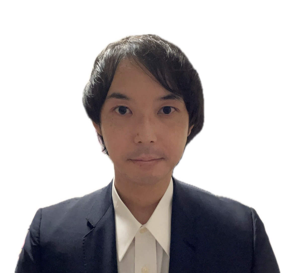
Invited Speaker
Speaker: Sotetsu Saito, R&D Engineer, Sony Semiconductor Solutions Corporation
Bio:
Sotetsu Saito joined Sony Semiconductor Solutions Corporation in 2014 and has been engaged in research and development of wafer bonding technologies. His recent work mainly focuses on Chip-on-Wafer hybrid bonding for CMOS image sensor applications
Abstract:
This presentation introduces the challenges of CoW hybrid bonding associated with the scaling of Sony’s CIS hybrid bonding to finer pitches. Based on recent research results, it discusses the understanding of bonding misalignment behavior and countermeasures for Cu recess. In addition, the electrical characteristics after CoW hybrid bonding with a 1.4 µm pad pitch are presented.
|
|
Development of Glass-Core Multilayer Build-Up Substrate with TGV
發表編號:S4-2時間:10:34 - 10:58 |
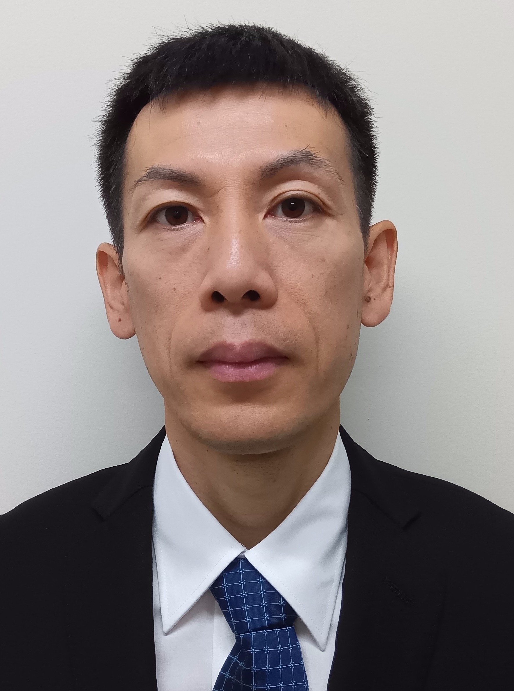
Invited Speaker
Speaker: Jun Yoshiike, , Shinko Electric Industries co., LTD
Bio:
Jun Yoshiike joined Shinko Electric Industries Co., Ltd. in 2003 and has been engaged in the research and development of next-generation semiconductor packaging technologies. His recent work mainly focuses on the development of multilayer package substrates using glass cores incorporating Through Glass Vias (TGVs).
Abstract:
To address SeWaRe defects induced by the coefficient of thermal expansion (CTE) mismatch between glass and resin, stress-relief structures consisting of resin-filled corner regions and edge-protection materials were introduced into a glass-core build-up substrate. The proposed structures effectively mitigated stress concentration during dicing and chip assembly. As a result, a TGV-equipped glass-core package substrate with high-density copper wiring and 11 build-up layers on each side was successfully fabricated without SeWaRe defects.
|
|
Development of PVD Sputtering Technology and Equipment for Seed-Layer Formation in Through-Glass Vias for Advanced Packaging
發表編號:S4-3時間:10:58 - 11:22 |

Invited Speaker
Speaker: Hiroto Sasaki, R&D Engineer, ULVAC, Inc
Bio:
Since joining ULVAC’s research laboratory in 2019, Hiroto Sasaki has been involved in the development of copper (Cu) fine interconnect deposition technology for front-end semiconductor processes. Since 2025, he has shifted to the field of advanced semiconductor packaging, and is currently responsible for developing the metallization process for through-glass vias (TGVs) for package substrates, as well as sputtering equipment for high-coverage applications.
Abstract:
Advances in AI technology are increasing demand for higher-performance and lower-cost AI modules. As a result, semiconductor packages require larger formats, finer interconnects, and higher integration. Glass core substrates are gaining attention as a key technology to meet these demands.
A major challenge for glass core substrates is TGV metallization, where achieving both reliability and mass production capability remains difficult.
This presentation introduces ULVAC’s PVD sputtering technology and equipment for TGV seed-layer formation, focusing on adhesion, high purity, low contamination, and step coverage.
|
|
Enabling Next-Generation Packaging with AGC’s TGV Technologies
發表編號:S4-4時間:11:22 - 11:46 |
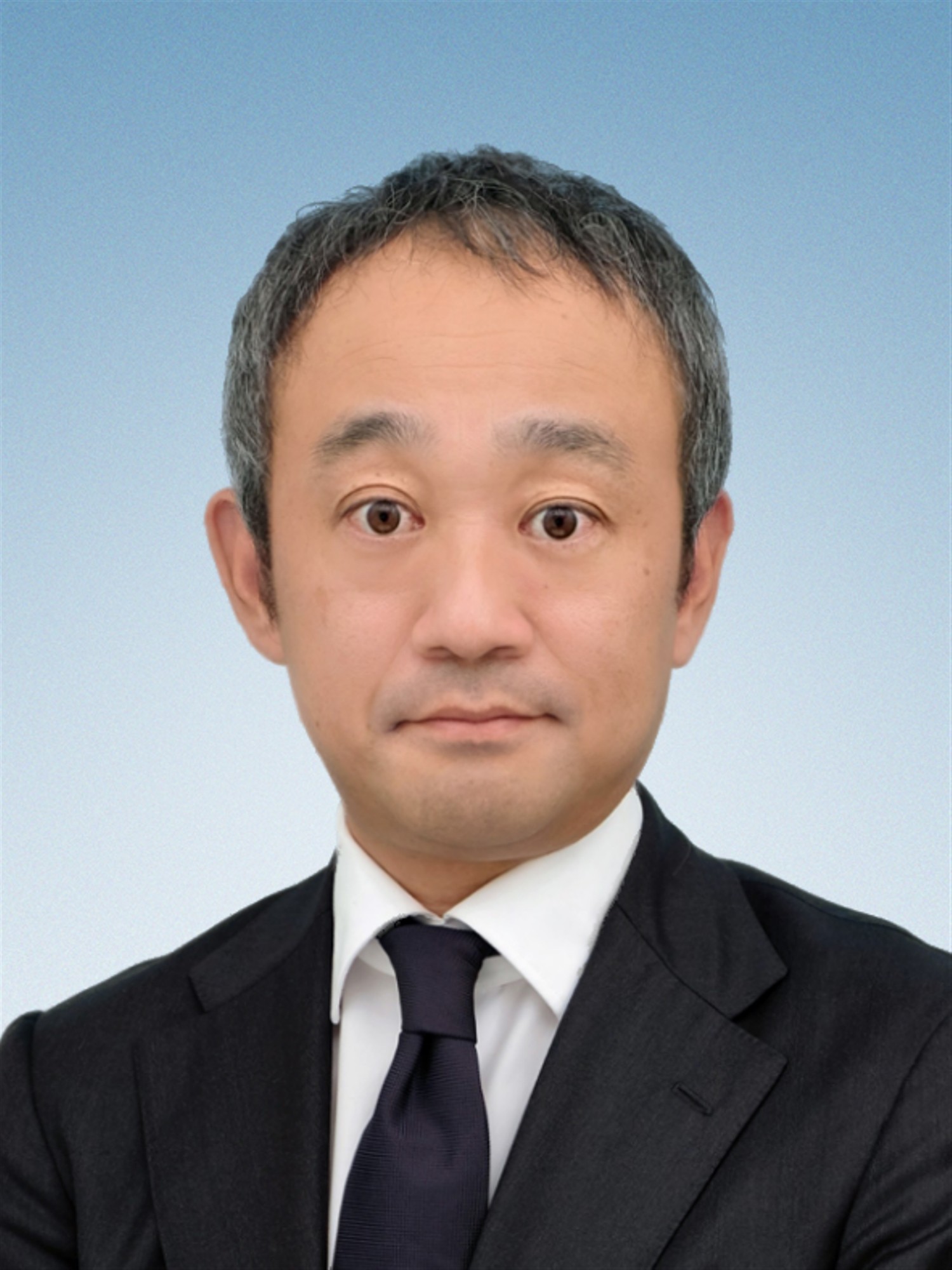
Invited Speaker
Speaker: Kohei Horiuchi, Senior Manager, AGC
Bio:
Kohei Horiuchi is a Senior Manager and Leader of Laser Team, Technology Development in the Advanced Semiconductor Packaging Group at AGC Inc. He leads the development of Through Glass Vias (TGV) technologies for next-generation semiconductor packaging and holds more than ten patents in this field. He received his master’s degree in Integrated Design Engineering from Keio University.
Abstract:
AGC’s TGV technology is a next-generation material solution that meets the electrical performance, thermal stability, and dimensional accuracy required for high-density, high-frequency packages. This presentation outlines the features of TGV processing technology and presents the results of electrical, thermal, and mechanical reliability evaluations, summarizing AGC’s contributions toward enabling next-generation packaging.
|
|
Fine Patterning Polyimide for RDL Dielectrics
發表編號:S4-5時間:11:46 - 12:10 |
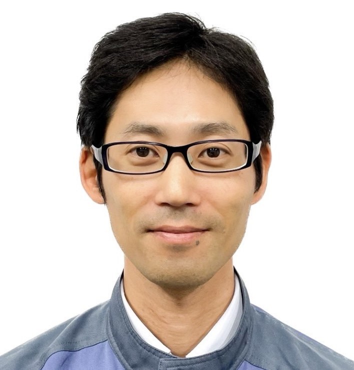
Invited Speaker
Speaker: Hitoshi Araki, Senior Research Manager, Toray Industries, Inc.
Bio:
Hitoshi Araki received master of degree from Kyoto University and joined Toray Industries in 2005. He moved to University of Illinois for research of flexible electronics from 2014 to 2016 by study abroad program of Toray. Returned to Toray in 2016, and from there to the present he has been involved in research on polyimides for semiconductor packaging. He received The Chemical Society of Japan Award for Technical Development in 2018.
Abstract:
With the advent of the AI era, the performance requirements for semiconductors and its packaging technologies have increased dramatically. In this technology trend, redistribution layers (RDLs) require materials and processes that offer higher functionality, higher density, and lower loss.
In this presentation, we introduce a high-resolution photosensitive polyimide developed by the authors. Furthermore, to enable finer patterning of high-performance polyimide, we also investigated a dry etching process using Photo-SOG as a mask, and the results will be presented.
|
|