S2 【S2】Enable Energy Efficient AI Technologies Through Integrated Material Solutions (Qnity)
Oct. 20, 2026 10:10 AM - 12:10 PM
Room: 701A, 7F, TaiNEX 2
Session chair: Lucy Wei, Advanced Circuit & Packaging, Qnity / Tim Tsai, Advanced Circuit & Packaging, Qnity
Thermal Challenges and Materials Solutions for Advanced Package in the AI Era
發表編號:S2-1時間:10:20 - 10:50 |
Invited Speaker
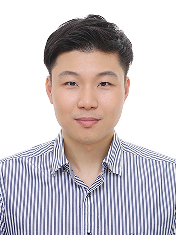
Speaker: Joungphil Lee, Principal Engineer, Techncial Leader, Samsung Electronics
Bio:
Joungphil Lee is a Principal Engineer and Part Leader of the Package Materials Development Group within the Advanced Process Development Team at Samsung Electronics. Joungphil Lee received a Ph.D. in Chemistry from Pohang University of Science and Technology (POSTECH) and completed postdoctoral research on conductive polymers for next-generation energy applications. Current work focuses on developing advanced materials for next-generation semiconductor packaging, including high-thermal-conductivity and glass-core materials.
Abstract:
The rapid expansion of AI is accelerating innovation in semiconductor packaging across both high-performance computing (HPC) systems and mobile devices. As power density and package complexity continue to increase, thermal management has become a key enabler for achieving high performance, energy efficiency, and long-term reliability. In other words, as the paradigm shifts toward mobile and on-device AI, thermal management at the package level is evolving from a design challenge to a fundamental physical limit.
This presentation will discuss the critical role of packaging materials in addressing the evolving thermal challenges of advanced AI packaging for both data center and mobile applications. Examples of material solutions, including the implementation of high thermal conductivity (high-k) materials and Heat Path Block (HPB) technologies for mobile AP and HBM packages, will be presented to illustrate how structural and material innovations have addressed increasingly demanding thermal requirements.
Building on these experiences, the presentation will explore the next generation of material solutions required as the industry moves toward package-level cooling for future HPC systems. Key enabling material technologies for these cooling architectures will be discussed, together with the structural and material innovations needed to support kilowatt-level power while maintaining package reliability and improving energy efficiency. Finally, the presentation will provide perspectives on future material innovations that will enable low-power, high-efficiency AI technologies across diverse computing platforms.
|
|
Material Innovations Empowering Megawatt AI Data Centers: The Synergy of Advanced Packaging, CPO, and VPD Architecture
發表編號:S2-2時間:10:50 - 11:20 |
Invited Speaker
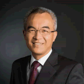
Speaker: Scott Chen, Senior Vice President, ASE Inc.
Bio:
Education:
Master of National Taiwan University (NTU) Executive MBA Program
B.A.of Chemical Engineering at NTU
Experience:
Sr. VP of Central Development Engineering in ASE since 2015
Staff Engineering Manager at Motorola Electronics Taiwan. (1999)
Process Engineer in Texas Instruments Taiwan.
Vice Chairman of MEMS Committee , Taiwan Semiconductor Industry Association (2013-2014)
Supplier-chain committee Chair of HiSPA ( Heterogeneously Integrated Silicon Photonics Alliance ) since 2024
Abstract:
As the generative AI boom drives individual data center racks toward megawatt-scale power densities, next-generation high-performance computing (HPC) clusters are confronting insurmountable physical barriers defined by the "bandwidth wall" and the "power wall."
this presentation explores an enabling framework of energy-efficient AI technologies based on a dual-axis system architecture: Co-Packaged Optics (CPO) connection solutions and Vertical Power Delivery (VPD) networks, seamlessly integrated through advanced packaging material innovations.
On the optical axis, CPO mitigates high-frequency signal loss by heterogeneously integrating optical engines with computing silicon, significantly shortening electrical trace lengths.
On the power axis, VPD addresses the physical limitations of legacy delivery systems by utilizing backside power delivery and through-silicon vias (TSVs) to route power vertically from integrated voltage regulators (IVRs) directly beneath the core logic. We systematically analyze the material reliability of high-current density power SiP modules under 800V DC server power architectures.
Ultimately, this work outlines a cohesive, multi-dimensional material optimization blueprint essential for unlocking the co-design of optical paths and vertical power topologies in 2030 AI infrastructure.
|
|
Advanced Copper Metallization Solutions for AI-Driven HDI
發表編號:S2-3時間:11:20 - 11:45 |
Invited Speaker
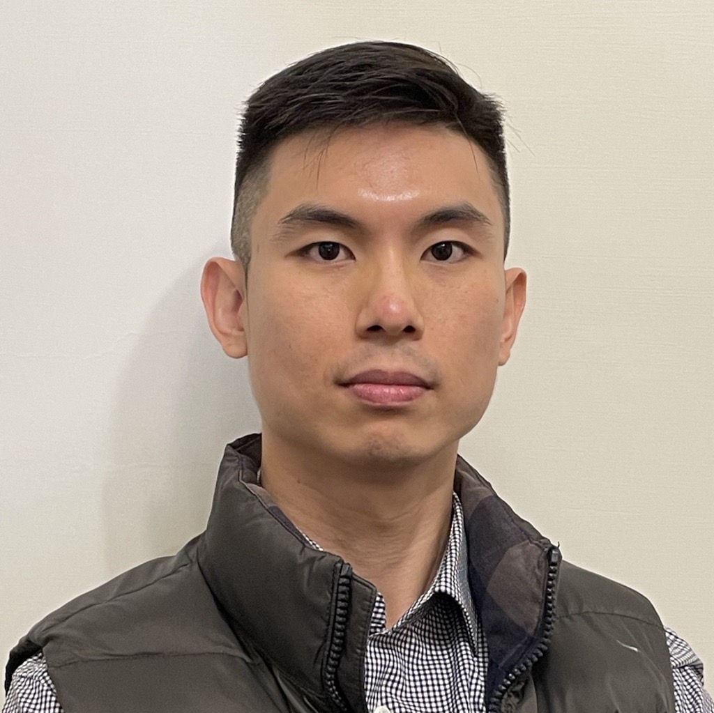
Speaker: Tim Lin, Lab Innovation Lead for Electroplating, R&D, Qnity
Bio:
Dr. Tim Lin is the Lab Innovation Lead for the Electroplating Segment within the metallization team of Advanced Circuit & Packaging at Qnity. In his current role, he leads efforts to advance laboratory capabilities that accelerate product development and enable rapid innovation for the fast-growing AI ecosystem.
In addition to leading laboratory innovation initiatives, Dr. Lin drives the development of next-generation electroplating solutions for advanced packaging applications. His work spans both mSAP technologies, where he focuses on enhancing void performance and superior via-filling capability for high-performance optical modules, and CoWoS-L technologies, which demand exceptional via-filling performance to support increasingly complex packaging architectures. Under his technical leadership, Qnity's mSAP products have achieved significant adoption among key customers, while the company's CoWoS-L solutions have earned critical recognition from leading industry players.
Dr. Lin holds a Ph.D. in Materials Science and Engineering from the Georgia Institute of Technology. His expertise encompasses electroplating chemistry, advanced metallization processes, and innovation strategies for semiconductor packaging technologies that power the next generation of AI computing platforms.
Abstract:
AI infrastructure is increasing the electrical, thermal, and reliability demands placed on HDI boards and advanced package substrates. Higher interconnect density, finer routing, and more complex build-up/core architectures are pushing copper metallization beyond conventional design windows, particularly for high-aspect-ratio blind via filling, through-hole conformal plating, and reliable electroless copper seed-layer formation. This presentation discusses Qnity’s integrated copper metallization approach for future AI-driven interconnect development, balancing Microfill™ EVF series acid copper, Copper Gleam™ PPR series pulse acid plating copper, and Circuposit™ 6900 electroless copper technologies across HDI and advanced package substrate use cases.
The Microfill™ EVF series acid copper is positioned for copper electroplating of high-aspect-ratio blind vias, targeting AR up to 1.5 while enabling void-suppressed filling, controlled dimple/bump profiles, and process optimization across feature size, plating thickness, and bath condition. The Copper Gleam™ PPR series pulse acid plating copper addresses through-hole conformal plating and throwing power requirements where board thickness, via geometry, and current distribution increasingly challenge uniform copper deposition. By applying pulse-reverse waveform control and bridge/fill process concepts, the Copper Gleam™ PPR series pulse acid plating copper supports metallization in demanding multi-layer boards configuring beyond 6.5 mm in depth with aspect ratio larger than 30. Circuposit™ 6900 electroless copper complements these electrolytic solutions through electroless copper metallization, supporting continuous, adherent seed-layer formation on advanced laminate systems and enabling downstream copper electroplating and via-fill reliability.
Reliability validation is central to this approach. Test vehicles are designed and fabricated to represent emerging AI infrastructure requirements, then characterized through cross-section inspection, process metrics, and external reliability testing. OM Thermal Stress Test (Object Measurement / Optical Modification System) validation conducted at Robisan Laboratory, Inc. is incorporated as an independent reliability reference, without overstating results beyond available data.
Beyond individual chemistries, the work highlights Qnity’s capability to combine test vehicle design, fabrication, reliability characterization, analytical metrology, and data-driven customer collaboration. This integrated framework connects material/process learning to customer design rules and supports scalable interconnect development for HDI, advanced package substrates, and next-generation AI electronics.
|
|
Enhancing Thermal Performance for Thin, High-Power PCBs for AI Data Centers
發表編號:S2-4時間:11:45 - 12:10 |

Invited Speaker
Speaker: Jake Joo, Global Technology Director, Advanced Flex Technologies, Qnity
Bio:
Jake Joo is the Global Technology Director for Advanced Flex Technologies (AFT) at Qnity, where he leads global technology strategy, advanced materials innovation, and new product development for rigid and flexible electronics. He is responsible for the company's worldwide R&D and application development organizations supporting the Kapton® polyimide films and Pyralux® laminate portfolio, working closely with customers and industry partners to develop next-generation materials solutions for consumer electronics, AI and high-performance computing, industrial systems, and emerging technologies.
Dr. Joo received his Ph.D. in Materials Science and Engineering from the Massachusetts Institute of Technology (MIT). Throughout his career, he has held a range of technical and leadership roles spanning semiconductor, interconnect, and electronic materials technologies, helping bring innovative materials solutions from research and development to commercial adoption. In addition to his industry leadership, he serves as a Board Member of the Advanced Photonics Coalition, contributing to the advancement of next-generation optical interconnect technologies that enable high-speed computing and data infrastructure.
Abstract:
The rapid growth of artificial intelligence (AI) and high-performance computing (HPC) is driving a fundamental transformation in power delivery architectures. As power density and current demand continue to increase within increasingly compact system designs, thermal management has become a critical challenge for next-generation power PCBs. Conventional PCB materials are often unable to simultaneously meet the requirements for thermal conductivity, electrical insulation, mechanical reliability, and manufacturability, creating new demands for advanced material solutions.
This presentation discusses how advanced thermally conductive PCB material technologies can address these challenges by improving heat dissipation while maintaining compatibility with conventional PCB manufacturing processes. It will highlight key design considerations and application opportunities for AI power boards and other high-power electronic systems, demonstrating how optimized material platforms can improve thermal performance, system reliability, and overall design flexibility.
As a provider of advanced material solutions, Qnity works closely with customers and partners across the electronics value chain to accelerate product innovation and enable the next generation of AI power electronics.
|
|
|